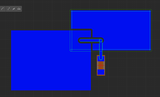
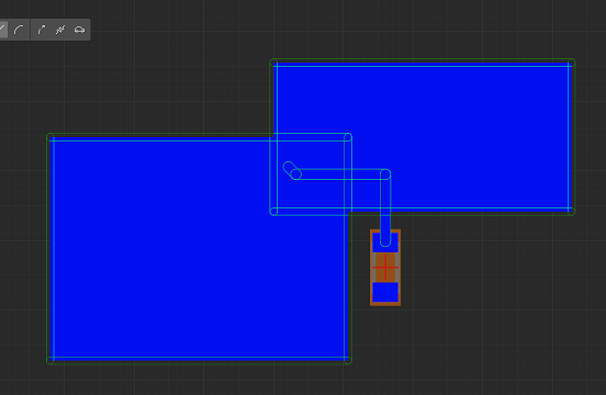
We have split our top ground pour in two, since our board requires different clearance distances applied to different sections of the board. We define them as overlapped. Even though the pours are associated with same named circuit (GND), we get a gap between the two pours.
None of the following settings appear to help:
- assigning same pour priority and re-pouring them simultaneously
- assigning different pour priorities and re-pouring them simultaneously
- manually re-pouring one after the other
- placing the pours adjacent to each other, ie back-to-back
- toggling the island removal
It appears the pour tool is incorrectly adding the clearance distance between the two pours when it processes the 2nd pour.
As a workaround we may be able to manually place wide copper traces that span the gap, however we are concerned PCB manufacturer’s CAD tools may not correctly handle the resulting Gerbers. (We need a continuous GND plane for RF).
Other suggestions or a path to get a fix?


